Mathematical fidelity: These page images preserve the exact notation and visual layout of the supplied PDF. The optional text extract below is for searching/copying only and may contain transcription errors.
Original pages — equations and symbols preserved
Show extracted text (searchable; equations may be imperfect)
Extract · PDF page 1
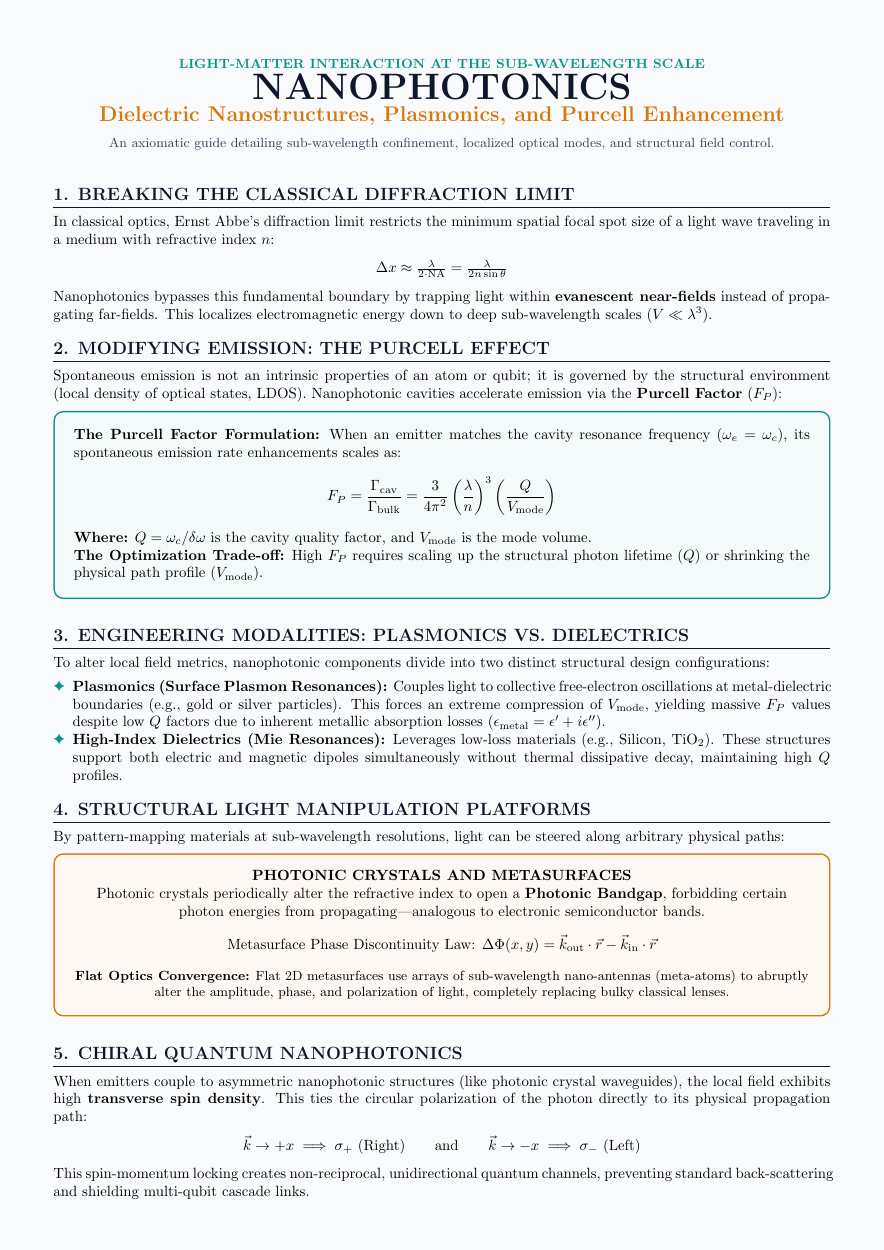
LIGHT-MATTER INTERACTION AT THE SUB-WAVELENGTH SCALE
NANOPHOTONICS
Dielectric Nanostructures, Plasmonics, and Purcell Enhancement
An axiomatic guide detailing sub-wavelength confinement, localized optical modes, and structural field control.
Extract · PDF page 1
1. BREAKING THE CLASSICAL DIFFRACTION LIMIT
In classical optics, Ernst Abbe’s diffraction limit restricts the minimum spatial focal spot size of a light wave traveling in
a medium with refractive index n:
∆x ≈ 2·NAλ = 2n sinλ θ
Nanophotonics bypasses this fundamental boundary by trapping light within evanescent near-fields instead of propa-
gating far-fields. This localizes electromagnetic energy down to deep sub-wavelength scales (V ≪λ3).
Extract · PDF page 1
2. MODIFYING EMISSION: THE PURCELL EFFECT
Spontaneous emission is not an intrinsic properties of an atom or qubit; it is governed by the structural environment
(local density of optical states, LDOS). Nanophotonic cavities accelerate emission via the Purcell Factor (FP ):
The Purcell Factor Formulation: When an emitter matches the cavity resonance frequency (ωe = ωc), its
spontaneous emission rate enhancements scales as:
Γcav 3 λ 3 Q
FP = =
Γbulk 4π2 n Vmode
Where: Q = ωc/δω is the cavity quality factor, and Vmode is the mode volume.
The Optimization Trade-off: High FP requires scaling up the structural photon lifetime (Q) or shrinking the
physical path profile (Vmode).
Extract · PDF page 1
3. ENGINEERING MODALITIES: PLASMONICS VS. DIELECTRICS
To alter local field metrics, nanophotonic components divide into two distinct structural design configurations:
✦Plasmonics (Surface Plasmon Resonances): Couples light to collective free-electron oscillations at metal-dielectric
boundaries (e.g., gold or silver particles). This forces an extreme compression of Vmode, yielding massive FP values
despite low Q factors due to inherent metallic absorption losses (ϵmetal = ϵ′ + iϵ′′).
✦High-Index Dielectrics (Mie Resonances): Leverages low-loss materials (e.g., Silicon, TiO2). These structures
support both electric and magnetic dipoles simultaneously without thermal dissipative decay, maintaining high Q
profiles.
Extract · PDF page 1
4. STRUCTURAL LIGHT MANIPULATION PLATFORMS
By pattern-mapping materials at sub-wavelength resolutions, light can be steered along arbitrary physical paths:
PHOTONIC CRYSTALS AND METASURFACES
Photonic crystals periodically alter the refractive index to open a Photonic Bandgap, forbidding certain
photon energies from propagating—analogous to electronic semiconductor bands.
Metasurface Phase Discontinuity Law: ∆Φ(x, y) = ⃗kout · ⃗r −⃗kin · ⃗r
Flat Optics Convergence: Flat 2D metasurfaces use arrays of sub-wavelength nano-antennas (meta-atoms) to abruptly
alter the amplitude, phase, and polarization of light, completely replacing bulky classical lenses.
Extract · PDF page 1
5. CHIRAL QUANTUM NANOPHOTONICS
When emitters couple to asymmetric nanophotonic structures (like photonic crystal waveguides), the local field exhibits
high transverse spin density. This ties the circular polarization of the photon directly to its physical propagation
path:
⃗k →+x =⇒σ+ (Right) and ⃗k →−x =⇒σ−(Left)
This spin-momentum locking creates non-reciprocal, unidirectional quantum channels, preventing standard back-scattering
and shielding multi-qubit cascade links.